General
How GPUs Run 36 Trillion Calculations/sec
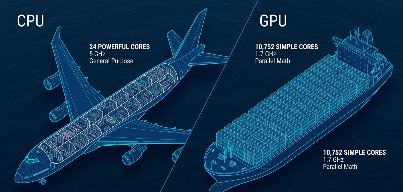
TL;DR Think of a CPU as a jumbo jet: fast, flexible, capable of landing at 40,000 different airports (meaning it can run any operating system, application, or hardware interface you throw at it). Its 24 cores are each highly sophisticated — they can handle complex branching logic,
Read this article as text (accessible version)
GPU Architecture Deep Dive
·
3,800 words · 4 interactive labs · April 2026
How GPUs Run
How GPUs Run
36 Trillion
Calculations/sec
Inside the chip that powers Cyberpunk 2077, ChatGPT, and Bitcoin — 28.3 billion transistors, 10,752 CUDA cores, and a computational architecture so parallel it would need 4,400 Earths full of humans to match. Here's exactly how it works.
Read the Deep Dive ↓ Open GPU Lab ⚡ 28.3B Transistors 10,752 CUDA Cores 35.6 TFLOPS Peak Performance 1.15 TB/s Memory Bandwidth 336 Tensor Cores Table of Contents- GPU vs CPU: Ships vs Airplanes
- GA102 Chip Architecture
- CUDA Core Design & FMA
- Chip Binning & Defect Tolerance
- GDDR7 Memory & PAM-3 Encoding
- SIMD: Embarrassingly Parallel
- SIMT: Warps & Thread Blocks
- Tensor Cores & Neural Networks
01GPU vs CPU: The Ship vs Airplane Argument
Here's the question that confuses almost everyone buying a gaming PC: a modern GPU has over 10,000 cores while a high-end CPU has maybe 24. So the GPU is obviously more powerful, right? It depends entirely on what you mean by "powerful" — and the answer reveals something fundamental about how computation actually works.
Think of a CPU as a jumbo jet: fast, flexible, capable of landing at 40,000 different airports (meaning it can run any operating system, application, or hardware interface you throw at it). Its 24 cores are each highly sophisticated — they can handle complex branching logic, manage network connections, run databases, and execute the kind of sequential decision-making that most software requires. A CPU core runs at 3-5 GHz and has enormous amounts of supporting hardware — branch predictors, out-of-order execution engines, large L3 caches — all designed to execute a single stream of complex instructions as fast as physically possible.
A GPU is a cargo ship: slower per individual movement, but capable of transporting vastly more at once. Its 10,000+ cores are each much simpler — essentially basic calculators that can multiply and add numbers. No branch prediction, no out-of-order execution, no running email clients. But when you need to perform the same arithmetic operation across millions of pieces of data simultaneously — like transforming every vertex in a 3D scene, or computing the activation of every neuron in a neural network — the GPU's sheer parallelism wins by a factor of hundreds. The key insight: GPUs win when the problem is "many independent calculations with the same operation." CPUs win when the problem is "complex sequential logic with lots of branching."
⚠️ The Cores Comparison Is MisleadingWhen GPU marketing says "10,000+ cores" versus a CPU's "24 cores," it's comparing fundamentally different things. A single CPU core has orders of magnitude more transistors devoted to control logic than a GPU core. A GPU core is essentially just an FMA unit — one multiplier, one adder. A CPU core contains entire prediction pipelines, out-of-order schedulers, and speculative execution hardware. A fair comparison would look at specific workloads: for matrix math, the GPU wins by 100×. For running an operating system or a database, the GPU can't even participate — it requires a CPU host to manage it.
02The GA102 Chip: A Hierarchy of 28.3 Billion Transistors
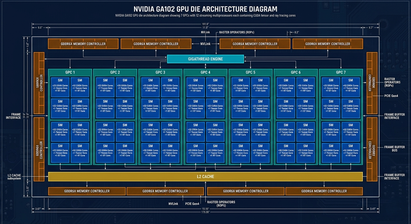
At the heart of NVIDIA's RTX 3090 is a chip called the GA102, etched at Samsung's 8nm node and containing 28.3 billion transistors — roughly 3.5 transistors per cell in your body. The vast majority of that die area is devoted to a strictly hierarchical processing structure. Understanding this hierarchy is the key to understanding how a GPU manages to keep 10,000+ cores all fed with work simultaneously.
The chip is organized into 7 Graphics Processing Clusters (GPCs). Inside each GPC are 12 Streaming Multiprocessors (SMs). Inside each SM are 4 warps, each containing 32 CUDA cores and 1 Tensor core, plus 1 Ray Tracing core per SM. Multiplying up: 7 GPCs × 12 SMs × 4 warps × 32 CUDA cores = 10,752 CUDA cores total. There are also 84 Ray Tracing cores (one per SM) and 336 Tensor cores (one per warp). These three core types handle three completely different workloads: CUDA cores run traditional shader math for game rendering, Tensor cores accelerate matrix multiplication for AI, and Ray Tracing cores accelerate the geometric intersection tests that make photorealistic lighting possible.
Around the edges of this compute fabric are 12 memory controllers connecting to the GDDR6X memory chips, plus the NVLink and PCIe interfaces. At the bottom of the die sits a 6 MB Level 2 SRAM cache, and there's the Gigathread Engine — the scheduler that decides which streaming multiprocessor gets which thread blocks. The Gigathread Engine is what makes the GPU feel "smart" despite its simple cores: it dynamically maps available work to available compute resources, hiding the latency of memory fetches by switching to a ready warp while another warp waits for data.
💡 Why the SM is the Real Unit of GPU ArchitectureDevelopers and researchers often talk about GPU performance in terms of Streaming Multiprocessors, not individual CUDA cores. An SM is the fundamental schedulable unit: it has its own L1 cache (128KB shared), its own register file, its own warp scheduler, and manages up to 2,048 active threads simultaneously through context switching. The CUDA programming model exposes thread blocks which map to SMs. Understanding the SM is more useful than counting raw CUDA cores because the SM's resource limits — registers, shared memory, warps — determine how many thread blocks can actually run concurrently.
03CUDA Core Design: A 410K-Transistor Calculator That Does One Thing Well
Zoom into a single CUDA core and the architecture is almost anticlimactic in its simplicity. About 410,000 transistors form a circuit whose primary function is FMA — Fused Multiply-Add: compute A × B + C in a single clock cycle. This operation, seemingly trivial, is the backbone of 3D graphics. Every vertex transformation, every texture sample blend, every lighting calculation reduces to combinations of multiply and add. The "fused" part matters: by combining the multiply and add into a single operation without rounding in between, you get better floating-point accuracy for the same silicon area.
Half the CUDA cores in the GA102 execute FMA on 32-bit floating-point numbers (FP32), which is essentially scientific notation with 23 bits of mantissa — more than enough precision for graphics calculations. The other half can switch between FP32 and INT32 (integer math), useful for memory address calculations and loop counters. For more exotic math — division, square root, trigonometric functions — the GPU has Special Function Units (SFUs), but only 4 of them per SM. This is fine for graphics workloads (you don't compute sin() on millions of vertices), but it means heavy transcendental math can become a bottleneck.
The math to understand why 36 trillion calculations per second is achievable: 10,496 CUDA cores × 2 operations per clock (one multiply + one add in FMA) × 1.7 GHz clock = 35.6 × 10¹² operations per second. That's it. 36 trillion calculations comes from running 10,000+ simple arithmetic units as fast as transistors physically allow. The GPU's secret isn't complex instruction sets or clever prediction logic — it's raw, repetitive, parallel arithmetic at enormous scale.
🔮 Myth: GPU Clock Speed Is All That MattersMarketing sometimes compares GPUs by clock speed alone: "This GPU runs at 2.5 GHz while that one runs at 1.7 GHz, so it's 47% faster!" But this completely misses the point. A GPU with 8,000 cores at 2.5 GHz has 20 TFLOPS. A GPU with 16,000 cores at 1.7 GHz has 54 TFLOPS — nearly 3× faster at the same actual work, despite a lower clock. Performance = (cores) × (operations per clock) × (clock frequency). Clock frequency is only one of three multipliers, and often the least important one for parallel workloads.
gpu_tflops_calc.py# Calculate theoretical GPU TFLOPS
def tflops(cuda_cores, clock_ghz, ops_per_cycle=2):
"""
ops_per_cycle=2 because FMA counts as 2 ops:
one multiply + one add per clock per core.
"""
total = cuda_cores * ops_per_cycle * clock_ghz * 1e9
return total / 1e12
# NVIDIA Ampere cards — same GA102 chip, different configs
cards = {
"RTX 3090 Ti": (10752, 1.86), # 40 TFLOPS — all cores enabled
"RTX 3090": (10496, 1.70), # 35.6 TFLOPS
"RTX 3080 Ti": (10240, 1.67), # 34.1 TFLOPS
"RTX 3080": (8704, 1.71), # 29.8 TFLOPS — 16 SMs disabled
}
print(f"{'Card':<16} {'Cores':>8} {'GHz':>6} {'TFLOPS':>8}")
print("-" * 42)
for name, (cores, ghz) in cards.items():
tf = tflops(cores, ghz)
print(f"{name:<16} {cores:>8,} {ghz:>6.2f} {tf:>7.1f}")
# RTX 3090 Ti 10,752 1.86 40.0 TFLOPS
# RTX 3090 10,496 1.70 35.7 TFLOPS
# RTX 3080 Ti 10,240 1.67 34.2 TFLOPS
# RTX 3080 8,704 1.71 29.8 TFLOPS
# All from same GA102 die — just different defect levels!
04Chip Binning: Why the RTX 3080 and 3090 Ti Are the Same Chip
Here's one of the most counterintuitive facts in the GPU industry: the RTX 3080, 3080 Ti, 3090, and 3090 Ti all use the identical GA102 chip design. The same photomask, the same transistor layout, the same silicon. The difference in performance and price comes entirely from how many cores survived manufacturing without defects.
Semiconductor manufacturing at 8nm is extraordinarily precise, but not perfect. Dust particles, photolithography errors, and random atomic-scale defects will inevitably damage some transistors during fabrication. Instead of throwing away the entire $600 chip because a few of 28.3 billion transistors are dead, engineers test each die, locate the defective streaming multiprocessors, and permanently disable those SMs via laser fuses. This process is called chip binning. A GA102 with all 84 SMs functional becomes a 3090 Ti. One with 80 working SMs becomes a 3090 (10,496 CUDA cores = 82 SMs × 128 cores). One with 16 disabled SMs becomes a 3080 (68 SMs × 128 = 8,704 cores).
The genius of this design is that NVIDIA's hierarchical, repetitive architecture makes binning work beautifully. Because every SM is identical, a defect in one SM only affects that SM's 128 CUDA cores — it doesn't corrupt any neighboring circuitry. The chip can be disabled at the SM granularity with no side effects. This dramatically improves chip yield (the percentage of usable dies per wafer), which is the dominant cost driver in chip manufacturing. Binning also means that when NVIDIA has higher production volume and fewer defects, they can offer more high-bin chips and retire lower-tier products — which is exactly what happened over the life of Ampere.
✅ Pro Tip: Binning Means Unlocking Is Sometimes RealIn rare cases, disabled SMs can be re-enabled with modified drivers or BIOS flashing — especially if the SM was disabled not because of a real defect but because NVIDIA needed to hit a specific product tier. This happened with several Ampere cards. However, attempting this voids warranties and can produce unstable cards (you might be enabling genuinely broken silicon). The safer play: buying a "lower tier" card with a fully enabled chip from an oversupply period often gives you a better price-to-core ratio than the premium tier.
05GDDR7 Memory & PAM-3: When Your GPU Stops Using Binary
GPUs are data-hungry machines. The RTX 3090 executes 35.6 trillion FMA operations per second — but those operations are useless if the cores are idle, waiting for data that hasn't arrived yet. This is why graphics memory (GDDR) engineering is as important as GPU core design, and why the gap between GPU memory bandwidth (1.15 TB/s) and CPU memory bandwidth (64 GB/s) is nearly 18:1.
The RTX 3090 uses 24 GB of GDDR6X memory across 12 chips, with a combined 384-bit bus width. Think of it as 12 parallel cranes all loading a cargo ship simultaneously — each crane moving 32 bits at a time, all running in parallel. The latest standard, GDDR7, goes even further by abandoning traditional binary signaling. Instead of wires that are either 0 V or 1 V (binary), GDDR7 uses PAM-3 (Pulse Amplitude Modulation, 3 levels) with voltages of −1, 0, and +1. Because each wire can now carry one of three states instead of two, you encode more bits per clock cycle. Specifically, GDDR7 converts 11 binary bits into 7 ternary digits — sending 276 binary bits worth of data using only 176 ternary symbols, a 36% efficiency improvement in signal bandwidth.
GDDR6X used PAM-4 (four voltage levels = 2 bits per symbol), but the industry decided PAM-3 was the better long-term standard for graphics memory. PAM-4 uses more distinct voltage levels, which makes the signal harder to distinguish — a receiver has to distinguish between 4 levels rather than 3, reducing noise margin. PAM-3 offers a better SNR (signal-to-noise ratio) at the same bandwidth improvement, making it easier to scale to higher frequencies without compromising signal integrity.
💡 The Real Bottleneck: Bandwidth, Not Clock SpeedGPU performance in real-world rendering is often memory bandwidth limited, not compute limited. A GPU with 35 TFLOPS but 400 GB/s bandwidth will perform similarly to one with 30 TFLOPS and 900 GB/s bandwidth on texture-heavy scenes — because the faster memory lets the compute units stay fed. This is why NVIDIA's workstation cards (like the A100) emphasize HBM memory with 2+ TB/s bandwidth over raw TFLOPS count. When your cores are waiting for data from memory, all those TFLOPS are wasted.
pam3_encoding.py# GDDR7 PAM-3 encoding: 11 binary bits → 7 ternary digits
# Efficiency gain: send 276 bits using only 176 trit signals
def bits_per_symbol(num_levels):
import math
return math.log2(num_levels)
binary_bps = bits_per_symbol(2) # classic: 1 bit per signal
pam4_bps = bits_per_symbol(4) # GDDR6X: 2 bits per signal
pam3_bps = bits_per_symbol(3) # GDDR7: ~1.58 bits per signal
# GDDR7's actual encoding trick: 11 bits → 7 trits
# (achieves better SNR than PAM-4 at similar bandwidth)
bits_encoded = 11
trits_used = 7
efficiency = bits_encoded / trits_used # 1.571 bits per trit
overhead_reduction = (1 - trits_used/bits_encoded) * 100
print(f"PAM-3 effective: {efficiency:.3f} bits/symbol")
print(f"Signal overhead reduced by: {overhead_reduction:.1f}%")
print(f"GDDR7 bandwidth gain vs binary: ~{(efficiency/binary_bps):.2f}×")
# Versus CPU's DRAM:
gddr_bw = 1150 # GB/s (384-bit bus GDDR6X)
dram_bw = 64 # GB/s (64-bit DDR5)
print(f"GPU/CPU bandwidth ratio: {gddr_bw/dram_bw:.0f}×")
06SIMD: Why Video Game Rendering Is "Embarrassingly Parallel"
Picture this: you're rendering a frame of Cyberpunk 2077. The scene contains 5,629 objects, each built from thousands of triangles defined by vertices in their own local "model space" coordinate system. Before any lighting or shading can happen, every single vertex — all 8.3 million of them — needs to be transformed from its object's local coordinate system into the shared "world space" coordinate system. That's 25 million addition operations. How do you schedule this?
With a CPU, you'd process vertices sequentially or with modest parallelism (24 cores). With a GPU, you use SIMD — Single Instruction, Multiple Data. The key insight: the transformation operation for vertex #1 and vertex #1,000,000 is identical. Add the object's world position to the vertex's local coordinates. Same instruction. Different data. There's no dependency between vertex 1's result and vertex 2's calculation — they're completely independent. This is what "embarrassingly parallel" means: no effort is needed to parallelize the problem because there are no data dependencies between tasks.
SIMD in practice: write a single shader program that transforms one vertex. Dispatch it to the GPU with "run this on all 8.3 million vertices." The GPU's Gigathread Engine maps those 8.3 million threads onto however many streaming multiprocessors are available, 32 threads at a time (a warp), running the same instruction on different vertex data simultaneously. Bitcoin mining works identically: run SHA-256 with the same transaction data but with a different nonce value for each of 95 million iterations — same instruction, different data, completely independent. Neural network forward passes also follow this pattern: compute activations for one sample in a batch versus another — independent, parallelizable, perfect for SIMD.
⚠️ SIMD Breaks Down With BranchingSIMD works beautifully when all threads run identical instructions. But what happens when some threads hit an if/else branch and go different directions? In pure SIMD, you have a problem called warp divergence: if 16 threads in a 32-thread warp execute the "if" branch and 16 execute the "else" branch, both branches must be serialized — the GPU masks off inactive threads and runs each branch sequentially. This can cut effective throughput by up to 50%. This is why GPU shaders are designed to minimize conditional branching, and it's one of the architectural problems that SIMT (the next section) addresses.
simd_vertex_transform.pyimport numpy as np
# SIMD: apply same transformation to all vertices simultaneously
# Model space → World space for a cowboy hat
hat_position_world = np.array([3.2, 1.0, -5.5]) # where hat is in world
# 14,000 vertices in model space (each with x,y,z)
vertices_model = np.random.randn(14000, 3) * 0.2 # hat is ~0.2m radius
# SINGLE INSTRUCTION: add world position to all model vertices
# This runs on all 14,000 vertices simultaneously on the GPU!
vertices_world = vertices_model + hat_position_world # broadcasting magic
# On CPU: loop over 14,000 vertices sequentially
# On GPU (SIMD): all 14,000 run in parallel across CUDA cores
# Scale: 5,629 objects × ~14,000 vertices = 78.8M transforms per frame
# At 60fps: 4.7 BILLION vertex transforms per second needed
print(f"Transforms per frame: {len(vertices_world):,} for hat alone")
print(f"Full scene (5629 objects): ~{5629*14000/1e6:.1f}M transforms/frame")
07From SIMD to SIMT: Warps, Thread Blocks, and the Jacquard Loom
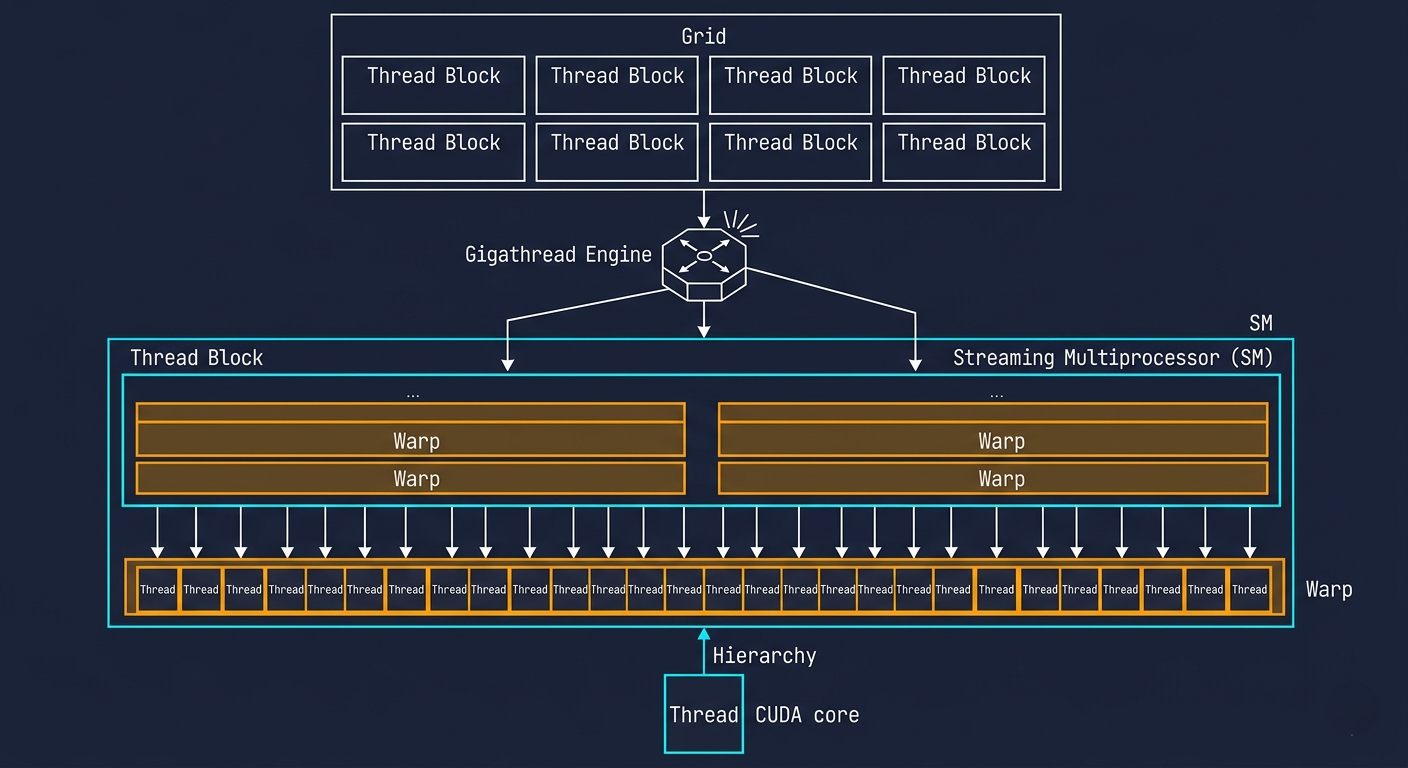
The execution model that maps SIMD compute onto the GPU's physical cores is called the thread hierarchy. A single computation task — transform one vertex — is a thread, assigned to one CUDA core. 32 threads executing the same program simultaneously form a warp. Multiple warps are grouped into a thread block, which the Gigathread Engine assigns to a streaming multiprocessor. Multiple thread blocks form a grid, which represents the entire workload for one GPU kernel call. The GPU's Gigathread Engine continuously monitors which SMs are available and dispatches thread blocks to keep all cores busy.
Until around 2016, NVIDIA GPUs used strict SIMD execution: all 32 threads in a warp had to execute the exact same instruction at the exact same time — in lockstep, like soldiers marching. This was efficient but brittle when code had conditional branches. Since Volta (2017), NVIDIA uses SIMT — Single Instruction, Multiple Threads. The key difference: each thread gets its own program counter, so individual threads within a warp can diverge and progress at different rates. They still share the same instruction scheduler and register file, but they're no longer forced to march in lockstep. SIMT also allows threads within an SM to share data through a 128 KB L1 cache — output from one thread can feed into another thread's computation. This makes SIMT dramatically more flexible for workloads with data-dependent branching, like certain image processing algorithms or graph traversal.
One historical footnote worth appreciating: the term "warp" doesn't come from Star Trek warp drives — it comes from the Jacquard Loom, invented in 1804. The loom used programmable punch cards to select specific "warp" threads (the lengthwise threads in weaving) and weave them together into complex patterns. The analogy to GPU warps — selecting threads, applying the same pattern — is not accidental. NVIDIA engineers clearly had an appreciation for the history of programmable parallel systems.
08Tensor Cores: The Matrix Multipliers Powering AI
Tensor cores represent a different design philosophy from CUDA cores. Where CUDA cores compute A × B + C on scalar (single) numbers, Tensor cores compute D = A × B + C where A, B, C, and D are entire matrices. The GA102 contains 336 Tensor cores, one per warp. A single Tensor core can compute a 4×4 matrix multiply-accumulate (MMA) in a single clock cycle — that's 64 multiply-add operations in the time it takes one CUDA core to do one.
Why does this matter for AI? Neural networks at every level — from the attention mechanisms in ChatGPT to the convolutional layers in image classifiers — reduce to matrix multiplication. A transformer layer's forward pass is essentially: input matrix × weight matrix, repeated thousands of times. Each layer of GPT-3 requires roughly 6 billion multiply-add operations per forward pass. At inference scale (millions of requests per day), the difference between using Tensor cores (with their 8× throughput advantage over CUDA cores for FP16 math) and not using them is the difference between a viable business and a loss-making one.
Tensor cores operate on smaller numerical formats than CUDA cores. While CUDA cores commonly use FP32 (32-bit float), Tensor cores shine with FP16 (16-bit), BF16, INT8, and even INT4 formats. The lower precision means each number occupies fewer bits, so you can fit more numbers into the same memory bandwidth — enabling even higher effective throughput. Modern LLM inference almost universally uses INT8 or FP16 quantization specifically to maximize Tensor core utilization and fit models into available VRAM.
💡 Tensor Cores Are Why NVIDIA Dominates AITensor cores are the primary reason NVIDIA's data center GPU revenue surpassed its gaming GPU revenue. The A100 has 312 TFLOPS of FP16 Tensor performance — 16× its FP32 CUDA performance. The H100 has 989 FP16 TFLOPS. This isn't cheating — FP16 is genuinely sufficient for neural network training and inference, and Tensor cores are specifically designed to deliver it. AMD and Intel have tried to compete with their own matrix accelerators (MI300, Gaudi), but NVIDIA's 10+ year head start in the CUDA ecosystem means most AI frameworks are natively optimized for Tensor cores, creating a software moat that's as important as the hardware advantage.
synthesisHow It All Connects
The story of a GPU runs from physics to software in one clean chain. At the transistor level, 28.3 billion switches form simple CUDA core circuits that compute A × B + C. These cores are organized hierarchically — warps of 32, SMs of 128, GPCs of 1,536 — with each level adding scheduling, caching, and coordination. The Gigathread Engine keeps all 84 SMs busy by swapping thread blocks. GDDR6X memory supplies 1.15 TB/s of data using PAM-4 multi-level signaling. SIMT lets thousands of threads execute the same shader program on different vertex data simultaneously. Tensor cores handle the matrix math that neural networks need at 8× the throughput of CUDA cores.
The same architecture that renders 60 frames per second of Cyberpunk 2077 also mines Bitcoin (SHA-256 is embarrassingly parallel), trains neural networks (matrix multiply on every layer), and runs inference for ChatGPT (Tensor cores + large batch sizes = maximum utilization). The GPU didn't become the universal compute engine by accident — its embarrassingly parallel architecture happens to match the structure of the most computationally demanding problems in modern computing.
getting startedProfile Your GPU with Real Tools
gpu_profiling.sh + python# ── 1. Check your GPU specs ─────────────────────────────────── nvidia-smi --query-gpu=name,memory.total,clocks.max.graphics \ --format=csv,noheader # ── 2. Monitor real-time utilization ───────────────────────── nvidia-smi dmon -s u # GPU + memory utilization per second # ── 3. Python: benchmark CUDA throughput ─────────────────────benchmark_gpu.py
import torch, time

# ── Benchmark CUDA core throughput (FP32) ────────────────────
device = torch.device("cuda")
N = 8192 # matrix size — large enough to saturate GPU
A = torch.randn(N, N, device=device, dtype=torch.float32)
B = torch.randn(N, N, device=device, dtype=torch.float32)

# Warm up GPU
torch.cuda.synchronize()
_ = torch.matmul(A, B)
torch.cuda.synchronize()

# Time 20 iterations
start = time.perf_counter()
for _ in range(20):
 C = torch.matmul(A, B)
torch.cuda.synchronize()
elapsed = time.perf_counter() - start

flops_per_matmul = 2 * N**3 # N^3 multiply-add pairs
tflops = (20 * flops_per_matmul) / elapsed / 1e12
print(ff"Achieved throughput: {tflops:.1f} TFLOPS (FP32)")

# ── Tensor Core throughput (FP16) ────────────────────────────
A_h = A.half(); B_h = B.half()
torch.cuda.synchronize()
start = time.perf_counter()
for _ in range(20):
 C_h = torch.matmul(A_h, B_h) # this hits Tensor Cores!
torch.cuda.synchronize()
tflops_h = (20 * flops_per_matmul) / (time.perf_counter()-start) / 1e12
print(ff"Achieved throughput: {tflops_h:.1f} TFLOPS (FP16/Tensor Cores)")
# Expected: FP16 ~4-8× faster than FP32 on Ampere (Tensor Core speedup)
FAQFrequently Asked Questions
Why can't a GPU run an operating system? + GPUs lack the hardware infrastructure that operating systems require. There's no interrupt controller to handle keyboard input, no DMA engine for network cards, no memory management unit that handles virtual memory for arbitrary processes, and no hardware support for the privilege levels (ring 0/ring 3) that let OSes safely isolate user programs from kernel code. GPUs also have no dedicated cache hierarchy for control flow — all their cache is designed for throughput (hiding memory latency for parallel warps), not latency (quickly responding to unpredictable events). The GPU is always a slave device controlled by a CPU host. Even CUDA programs run on the GPU only after a CPU program has set up buffers, copied data, and issued kernel launch commands through the CUDA runtime. What is the difference between VRAM and system RAM? + VRAM (Video RAM, technically GDDR memory) and system DRAM differ in three key ways: bandwidth, physical placement, and purpose. VRAM has an 18× wider memory bus (384-bit vs 64-bit for DDR5) and sits directly on the GPU's circuit board, connected to the GPU chip via short copper traces. This gives it ~1 TB/s bandwidth. System DRAM uses a narrower bus (64-bit per channel) and connects to the CPU via the motherboard, achieving ~64-128 GB/s for consumer systems. VRAM is also typically less dense (lower total capacity) and more expensive per GB because the wide bus requires more physical pins. The fundamental reason GPUs need high-bandwidth memory is that CUDA cores can perform math 18× faster than CPU cores can — so their memory must supply data 18× faster too, or the cores starve. Why did Bitcoin mining move from GPUs to ASICs? + An ASIC (Application-Specific Integrated Circuit) is a chip designed to do exactly one thing — in this case, compute SHA-256 hashes. Because every transistor on the chip is dedicated to that specific function, an ASIC can be vastly more efficient than a GPU doing the same calculation on its general-purpose FMA units. Modern Bitcoin ASICs achieve 250 trillion hashes per second — equivalent to 2,600 RTX 3090s — at a fraction of the power consumption per hash. GPUs won the early Bitcoin mining era because SHA-256 is embarrassingly parallel and GPUs were the best readily available parallel compute hardware. ASICs ended that era around 2013-2014 by offering a 100-1000× efficiency advantage. Today, GPU mining is economically viable only for cryptocurrencies that deliberately design their proof-of-work algorithms to be ASIC-resistant (like using large memory requirements that ASICs can't easily satisfy). What is the difference between CUDA cores and Tensor cores in practice? + CUDA cores operate on individual numbers (scalars): compute A × B + C where A, B, C are single floating-point values. Tensor cores operate on matrices: compute D = A × B + C where A is 4×4, B is 4×4, C is 4×4, and D is 4×4 — computing 64 multiply-add operations per clock cycle per Tensor core. In practice, CUDA cores handle all traditional GPU rendering work: vertex shading, texture sampling, pixel shading, and general compute kernels that don't involve large matrix operations. Tensor cores handle deep learning (forward passes, gradient computation), certain image upscaling algorithms (like DLSS which uses a neural network), and any compute task that can be expressed as batched matrix multiplications. A single Tensor core has ~8× the throughput of a CUDA core for the same silicon area when doing matrix math. How does chip binning affect GPU pricing? + Chip binning creates a natural price hierarchy from a single chip design. NVIDIA sets prices so that lower-bin chips (more defects → fewer working cores) sell at lower prices, subsidizing the cost of the manufacturing process while still selling chips that would otherwise be wasted. The economics are complex: higher-bin chips (3090 Ti) command premium prices because they're rarer — not every wafer produces many flawless dies. Lower-bin chips (3080) are more abundant and cheaper. This also means "buying the dip" with lower-tier cards can be surprisingly good value: the 3080's 8,704 cores came from the same fundamentally capable GA102 die as the 3090's 10,496 cores, just with more disabled SMs. What is HBM memory and why does it matter for AI? + HBM (High Bandwidth Memory) stacks multiple DRAM dies vertically and connects them with through-silicon vias (TSVs) — essentially drilling holes through the silicon and running wires through them. A single HBM3E stack can have up to 36 GB of memory with bandwidths of 1.2+ TB/s per stack, and you can place 4-8 stacks around an AI accelerator chip. The H100 SXM uses 5 HBM3 stacks for 80 GB total at 3.35 TB/s bandwidth. This matters for AI because large language models like GPT-4 have hundreds of billions of parameters that need to flow through the chip during inference. A model with 70 billion FP16 parameters weighs 140 GB — already exceeding single-GPU GDDR memory. HBM's higher density and bandwidth make it the only viable memory technology for frontier AI model inference. Why do newer GPUs use smaller numbers (FP8, INT4) for AI? + Lower-precision formats pack more numbers into the same memory bandwidth, which is the primary bottleneck for LLM inference. If you switch from FP32 (4 bytes per number) to FP8 (1 byte per number), you can move 4× as many model weights through the memory bus per second — meaning your Tensor cores stay fed with data rather than waiting for memory. The precision loss from FP8 or INT4 quantization is generally acceptable for inference (though less so for training) because neural network weights have natural redundancy: many weights are near-zero and can be rounded aggressively without significantly affecting output quality. NVIDIA's H100 introduced FP8 Tensor core support for exactly this reason — it delivers up to 2× the effective throughput of FP16 for inference workloads. Can you run AI workloads on gaming GPUs instead of professional AI GPUs? + Yes, with caveats. Gaming GPUs (RTX 4090 etc.) have the same Tensor core architecture as professional GPUs (A100, H100) and can run PyTorch, TensorFlow, and most AI frameworks perfectly well. The key limitation is VRAM: a gaming RTX 4090 has 24 GB, while an H100 has 80 GB. Larger models that don't fit in 24 GB require multi-GPU setups or model sharding. Performance-per-dollar for training and inference on consumer GPUs is often excellent — the RTX 4090 delivers about 82 TFLOPS FP16 Tensor performance for ~$1,600, while an A100 delivers 312 TFLOPS for ~$10,000. For solo researchers and small teams, gaming GPUs with quantized models (using bitsandbytes or GGUF format) are the dominant choice for running frontier AI locally.⚡ GPU Lab
Four interactive experiments: build your own GPU, run SIMD transforms, do tensor core matrix math, and race GPU vs CPU.
Peak TFLOPS comparison — your GPU config vs real cards · log scale
GPU Performance Calculator CUDA Cores 10,496 Clock Speed (GHz) 1.70 GHz Precision 35.7 TFLOPS 1.0× vs RTX 3090 4,400 Earths of People Cyberpunk 2077 Equivalent GameFormula: TFLOPS = (CUDA cores × 2 ops/cycle × Clock GHz) / 1000. The "×2" comes from FMA: one multiply + one add per clock cycle per core.
SIMD vertex transform — yellow = pending · cyan = processing · green = done
SIMD Vertex Transform Simulator Vertices per Object 14,000 Number of Objects 100 Active CUDA Cores 10,496 1.4M Total Transforms — GPU Batches — GPU Time (est) — Speedup vs CPU Tensor Core Matrix Multiply-Accumulate: D = A × B + C Matrix A (4×4) × Matrix B (4×4) Matrix C (4×4) Result Matrix D (4×4) — computed by ONE Tensor Core in ONE clock cycle 64 Ops per Cycle 64 CUDA Cycles Needed 64× Tensor vs CUDA 336 × 64 Total Ops/Cycle (GPU)Each cell in D = sum of (row from A) dot (column from B) + C[i][j]. A Tensor Core computes all 16 output cells simultaneously, each requiring 4 multiplications + 3 additions + 1 accumulation = 8 ops per cell × 16 cells = 128 operations. At 1.7 GHz across 336 Tensor cores: 73 TOPS in FP16 mode.
GPU (cyan) vs CPU (orange) completing parallel tasks · same total work, different parallelism
GPU vs CPU Race Simulator Total Work Units 100,000 GPU Cores 10,496 CPU Cores 24 CPU Core Speed Advantage 3.0× Task Type — GPU Time — CPU Time — Winner — SpeedupKeep reading
Related articles
 General
How Microchips Are Made: The Complete CPU Fabrication Process Step by Step | Zetsapp
Here's the thing most chip articles miss: the "nm" number in modern process node names (TSMC 3nm, Intel 4nm, Samsung 3nm) does not correspond to any physical dimension on the chip. This was true when Intel's 45nm node launched in 2007 and became increasingly disconnected from reality thereafter. TSMC's "3nm" node has a gate pitch (the distance between gates) of approximately 48nm — not 3nm.
 General
How Hard Disk Drives Work: Inside the Spinning Metal That Still Stores Most of the Internet | Zetsapp
Here's the thing most explainers skip: that internal air isn't just "kept clean," it's engineered. Traditional HDDs are filled with filtered, dry air at roughly atmospheric pressure because the read/write head relies on aerodynamic lift from that specific air density to fly at the correct height — too thin an atmosphere and the head flies too low or crashes; too thick and it flies too high to read reliably.
 General
How GPUs Actually Work: The Nvidia GA102 Architecture Decoded Inside the RTX 3090
GPU acceleration is limited by the fraction of your workload that's actually parallel. Amdahl's Law states: if 90% of a program can be parallelized, the maximum speedup from infinite parallel processors is 10× — not infinite. The 10% sequential bottleneck always limits total speedup. In GPU-accelerated ML training, the actual workload split is typically: 85-95% embarrassingly parallel tensor operations