GPU-architectureNvidia-GA102CUDA-coresTensor-coresRTX-3090SIMTGDDR6Xchip-binningwarp-divergenceparallel-computing
General
How GPUs Actually Work: The Nvidia GA102 Architecture Decoded Inside the RTX 3090
TL;DR GPU acceleration is limited by the fraction of your workload that's actually parallel. Amdahl's Law states: if 90% of a program can be parallelized, the maximum speedup from infinite parallel processors is 10× — not infinite. The 10% sequential bottleneck always limits total speedup. In GPU-accelerated ML training, the actual workload split is typically: 85-95% embarrassingly parallel tensor operations
Read this article as text (accessible version)
// GPU Architecture · Nvidia GA102 · RTX 3090
·
4,000 words · 4 interactive labs · April 2026
How GPUs Actually Work:
How GPUs Actually Work:
The Nvidia GA102
Architecture Decoded
Inside the RTX 3090
You've run CUDA code, configured PyTorch to use your GPU, and watched your model train 50× faster than on CPU. But if someone asked you to explain exactly why — what happens inside the chip, why Tensor Cores make matrix math so fast, or why the same silicon die produces three different product tiers — could you answer? This is that guide.
Read the Deep Dive ↓ Open GPU Lab ⚡ 10,496 CUDA Cores 328 Tensor Cores (3rd gen) 84 RT Cores (2nd gen) 24GB GDDR6X · 936 GB/s SIMT · Warp Scheduling // Table of Contents- GPU vs CPU: Cargo Ship vs Jumbo Jet
- GA102 Physical Architecture
- Manufacturing & Chip Binning
- GDDR6X: The Data Pipeline
- SIMD to SIMT: Evolution of Parallelism
- Applications: Gaming, Mining & AI
A machine learning researcher at a biotech company had a frustration problem. Her protein folding model trained on CPU took 14 hours per run. After she bought an RTX 3090 and switched to GPU training, it took 18 minutes. The speedup was 46×. She understood that GPUs were faster for matrix math — everyone knows that now. What she didn't understand was why. Why does the same matrix multiplication that takes 8 seconds on a 32-core Threadripper take 400 milliseconds on a GPU? Why does a chip with 10,496 cores outperform a chip with 32 cores by 40×? And what exactly are those 10,496 "cores" doing that's so different from what a CPU core does?
The answers are in the silicon. The Nvidia GA102 chip powering the RTX 3090 is one of the most extensively documented pieces of semiconductor engineering in history — Nvidia published a 68-page whitepaper on its architecture. This guide distills that architecture into the concepts that actually matter for engineers using GPUs for gaming, AI, or high-performance computing.
// 01GPU vs CPU: The Cargo Ship and the Jumbo Jet
A CPU is a jumbo jet. It carries passengers (tasks) from point A to point B with incredible speed, sophistication, and individual attention to each passenger. It handles baggage for some, special meals for others, first-class upgrades for priority cases. It can navigate to almost any destination, respond to turbulence intelligently, and change course mid-flight. But it holds maybe 800 people and takes hours for each round trip. A GPU is a cargo ship. It's slower per unit of movement, it can only carry cargo (not passengers with complex needs), and it's not nimble. But it carries 200,000 shipping containers per trip, and every container gets exactly the same treatment — which is exactly what you want when you're moving 200,000 containers.
A modern CPU has 8-64 cores, each extraordinarily powerful. Each core has sophisticated branch prediction hardware (to guess which way an if-else statement will branch before evaluating the condition), out-of-order execution (executing instructions in whatever order maximizes pipeline utilization), large L1/L2/L3 caches, and deep instruction pipelines. These features exist because CPU workloads are control-flow intensive: web servers handle diverse requests, operating systems schedule heterogeneous processes, compilers make complex decisions based on code structure. Each CPU core needs to be fast and flexible because consecutive instructions are often different, interdependent, and conditional.
A GPU core is fundamentally simpler. It lacks branch prediction, out-of-order execution, and the deep caches that make CPUs so versatile. What it has instead is a ruthlessly optimized floating-point arithmetic pipeline. The GA102 has 10,496 CUDA cores — single-precision floating-point multiply-add units — that can all execute the same instruction simultaneously on different data. This is not just "many cores" — it's a fundamentally different execution model. When you multiply two 4096×4096 matrices, every output cell's dot product can be computed independently. The GPU assigns different output cells to different CUDA cores, computes all of them in parallel, and completes the operation in a fraction of the time a CPU requires processing them sequentially.
💡 The Amdahl's Law CaveatGPU acceleration is limited by the fraction of your workload that's actually parallel. Amdahl's Law states: if 90% of a program can be parallelized, the maximum speedup from infinite parallel processors is 10× — not infinite. The 10% sequential bottleneck always limits total speedup. In GPU-accelerated ML training, the actual workload split is typically: 85-95% embarrassingly parallel tensor operations (perfectly suited for GPU) and 5-15% data loading, preprocessing, and control logic (must run on CPU). This is why even the best GPU configurations still require a fast CPU and fast NVMe storage — the sequential bottleneck becomes the limiting factor when GPU compute is sufficiently fast.
cpu_vs_gpu_matmul.py — timing comparisonimport torch, time
N = 4096
A = torch.randn(N, N)
B = torch.randn(N, N)
# CPU benchmark
start = time.perf_counter()
C_cpu = torch.mm(A, B)
cpu_ms = (time.perf_counter() - start) * 1000
print(ff"CPU: {cpu_ms:.0f}ms") # → ~820ms (Ryzen 9 5950X)
# GPU benchmark (RTX 3090)
A_g, B_g = A.cuda(), B.cuda()
torch.cuda.synchronize() # wait for transfers
_ = torch.mm(A_g, B_g) # JIT warmup
torch.cuda.synchronize()
start = time.perf_counter()
C_gpu = torch.mm(A_g, B_g)
torch.cuda.synchronize() # GPU is async — must sync before timing
gpu_ms = (time.perf_counter() - start) * 1000
print(ff"GPU (CUDA cores): {gpu_ms:.0f}ms") # → ~4ms
# With Tensor Cores (via Automatic Mixed Precision)
with torch.amp.autocast('cuda'):
start = time.perf_counter()
C_amp = torch.mm(A_g.half(), B_g.half())
torch.cuda.synchronize()
amp_ms = (time.perf_counter() - start) * 1000
print(ff"GPU (Tensor Cores, FP16): {amp_ms:.0f}ms") # → ~0.8ms!
# → CPU: 820ms | CUDA: 4ms | Tensor: 0.8ms → 1000× over CPU
// 02GA102 Physical Architecture: A City of Specialized Districts
The GA102 die is 628mm² of silicon containing 28.3 billion transistors. Looking at it under a microscope or in Nvidia's architecture diagrams, you see a hierarchical structure that resembles a city divided into districts, each district containing specialized facilities. Understanding this hierarchy is the key to understanding how GPU programming works — because every level of the hierarchy corresponds to a level of abstraction in CUDA programming.
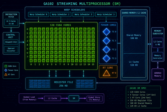
At the top level, the GA102 contains 7 Graphics Processing Clusters (GPCs) — the districts. Each GPC contains 6 Texture Processing Clusters (TPCs), and each TPC contains 2 Streaming Multiprocessors (SMs). The fully-enabled GA102 (as in the RTX 3090) has 84 SMs total (7 × 6 × 2). Each SM is the fundamental compute unit — the "factory" in our city analogy. And inside each SM is where the action happens: 128 CUDA cores (simple floating-point multiply-add units), 4 Tensor Cores (3rd generation, specialized for matrix math), 1 RT Core (2nd generation, specialized for ray-triangle intersection calculations), a register file (6MB), shared memory/L1 cache (128KB), and a warp scheduler that orchestrates all of this.
The three types of cores serve distinct purposes. CUDA cores are binary calculators — fast at single-precision (FP32) or integer (INT32) arithmetic. They're what runs your game's vertex shaders, applies post-processing effects, and executes general CUDA code. Tensor Cores are specialized matrix multiply-accumulate units. A single Tensor Core can perform a 4×4 matrix multiply in one clock cycle — a 64-FLOP operation that would take 64 sequential multiply-add operations on a CUDA core. This is what makes modern AI training and inference so fast on Ampere and later architectures. RT Cores handle bounding volume hierarchy traversal — the computational bottleneck in real-time ray tracing — in dedicated hardware so it doesn't consume CUDA or Tensor Core cycles.
The counterintuitive insight about GPU cores: they're not individually very fast. A single CUDA core runs at 1.7 GHz boost clock on the RTX 3090 and executes one multiply-add per cycle. A modern CPU core running at 5 GHz executes multiple instructions per cycle via superscalar execution and out-of-order mechanisms. The GPU's advantage isn't individual core speed — it's the number of cores and the efficiency with which they're kept busy on parallel workloads.
💡 The Warp: The GPU's Fundamental Execution UnitThe CUDA programming model talks about threads, but the hardware executes warps — groups of 32 threads that execute in lockstep. When your CUDA kernel launches 1000 threads, the SM's warp scheduler groups them into 32 warps of 32 threads each. All 32 threads in a warp execute the same instruction simultaneously (on different data). When a warp hits a memory access that takes 200+ cycles, the scheduler switches to another ready warp to keep the CUDA cores busy — this is called latency hiding. The RTX 3090's SMs can have up to 48 warps resident simultaneously per SM (1536 threads per SM), giving the scheduler many warps to switch between when one blocks. This latency-hiding through warp switching is fundamentally different from how CPU cores handle memory latency (through caches and out-of-order execution).
// 03Manufacturing & Chip Binning: Why the Same Die Becomes Three Products
Here's something that surprises many engineers: the RTX 3080, RTX 3080 Ti, and RTX 3090 all use the exact same GA102 silicon die — the same physical chip design, fabricated on the same TSMC 8nm process node. The differences between these products are entirely about which parts of that die are enabled and what VRAM configuration they ship with. This practice is called "chip binning," and it's one of the most economically important engineering decisions in semiconductor manufacturing.
Semiconductor fabrication is not perfect. When TSMC prints 28.3 billion transistors onto a 628mm² area of silicon using 8nm photolithography, some transistors will have defects — microscopic imperfections from dust particles, photolithography aberrations, or doping variations. A fully functioning GA102 die (all 84 SMs working) is the best-case scenario, but not every die comes out perfect. If 4 of the 84 SMs have defects that prevent them from functioning, the chip manufacturer doesn't throw the die away — they disable those 4 SMs in hardware (by burning fuses or adjusting configuration bits) and sell it as an RTX 3080 (which has 68 SMs enabled). If only 2 SMs are defective, it becomes an RTX 3080 Ti (80 SMs). If all 84 SMs are working, it can be sold as an RTX 3090 (84 SMs), which commands a higher price.
This also means Nvidia can intentionally produce lower-tier products from perfect dies when demand dictates. If the market needs more RTX 3080s than 3090s, Nvidia can take a perfect 84-SM die and disable 16 SMs to sell it as a 3080. The "waste" is intentional — better to sell at the 3080 price point than let the 3090 market saturate while 3080 demand goes unmet. This practice is economically rational and explains why the yield economics of semiconductors are so complex: what matters isn't just how many good chips come out, but how the distribution of partially-defective chips maps to the product lineup the market demands.
⚡ What This Means for Overclocking and UndervoltingChip binning has a practical implication for GPU tuning: some RTX 3080s are actually perfect 84-SM dies with SMs disabled in software. For a time in 2020-2021, enthusiasts discovered they could re-enable disabled SMs on some RTX 3080s (turning them into 3090s) by modifying BIOS configurations — Nvidia responded by changing the hardware fusing mechanism to make this impossible. The broader lesson: the silicon lottery isn't random. Chips that pass the full 84-SM specification get sold as 3090s; those that don't get sold cheaper. If you get an RTX 3080 that overclocks exceptionally well, there's a reasonable chance you got a chip that nearly passed full 3090 specs — the defects that disqualified it from 3090 binning may have been in the disabled SMs, not the enabled ones.
// 04GDDR6X: The Data Pipeline That Feeds 10,496 Hungry Cores
Imagine you've hired the fastest assembly workers in the world — 10,496 of them — and built them a state-of-the-art factory floor. Now imagine the loading dock is a single narrow alleyway that can only accept one truck at a time. Those workers will spend most of their time waiting for materials rather than assembling. This is the memory bandwidth problem for GPUs, and it's why the memory subsystem of a GPU is as important as the compute cores.
The RTX 3090's 24GB of GDDR6X memory delivers 936 GB/s of memory bandwidth — roughly 10× the bandwidth of DDR5 system RAM used by CPUs. This bandwidth is achieved through two mechanisms: physical width (the RTX 3090 has a 384-bit memory bus — essentially 384 parallel wires connecting the GPU die to the memory chips, vs 64-bit for system RAM) and advanced signaling (GDDR6X uses PAM4 — Pulse Amplitude Modulation with 4 signal levels — to transmit 2 bits per cycle per wire instead of 1, effectively doubling throughput without changing clock speed or bus width).
Memory bandwidth is the binding constraint for many GPU workloads — not compute. A workload is compute-bound if the CUDA/Tensor cores are the bottleneck (they're busy 100% of the time and adding memory bandwidth wouldn't help). A workload is memory-bound if the cores are waiting for data more than they're computing (memory bandwidth is the bottleneck). For transformer inference with large batch sizes, the workload is typically compute-bound — exactly what GPUs are designed for. For transformer inference with batch size 1 (single-user interactive queries), the workload is often memory-bound — the model weights must be loaded from VRAM for every token generated, and 24GB of weights takes time to stream through even 936 GB/s. This is why batching inference requests improves GPU utilization: it amortizes the weight loading cost across many queries.
⚠️ VRAM Capacity vs Bandwidth: Know Which You're Limited ByTeams frequently misdiagnose GPU performance problems by assuming more VRAM = faster inference. VRAM capacity determines how large a model can fit. VRAM bandwidth determines how fast data moves between memory and compute cores. These are independent constraints. A model that fits in VRAM but runs slowly may be memory-bandwidth-limited (solution: use smaller batch sizes that fit in L2 cache, or switch to a GPU with higher bandwidth like the H100's 3.35 TB/s HBM3). A model that doesn't fit in VRAM needs either more VRAM capacity or model parallelism (solutions: larger VRAM GPU, multi-GPU tensor parallelism, or 4-bit quantization to reduce model size). Use `nvidia-smi` to monitor both VRAM utilization and memory bandwidth utilization as separate metrics before diagnosing performance problems.
// 05From SIMD to SIMT: How Nvidia Unlocked True Thread-Level Flexibility
Early GPU programming was brutally rigid. The hardware executed in a model called SIMD — Single Instruction, Multiple Data — where every processing unit in a group had to execute exactly the same instruction at exactly the same time, on different data. This lock-step execution meant that if-else branches were catastrophically expensive: if half the threads in a group needed to take the "if" branch and half needed the "else," the hardware would execute both branches sequentially, masking the results for the threads not taking each branch. This "warp divergence" effectively serialized parallel code whenever branches were present.
Nvidia's SIMT — Single Instruction, Multiple Threads — is a crucial architectural evolution. While warps still execute in lockstep by default (all 32 threads execute the same instruction each cycle), SIMT gives each thread its own program counter and register state. This means threads within a warp can diverge independently: when a branch is encountered, diverged threads can be tracked separately and reconverged when the branch paths merge. More importantly, SIMT allows threads to stall at different points without blocking others — crucial for memory operations that may return at different times. The Volta architecture (2017) enhanced SIMT further with independent thread scheduling, allowing threads to reconverge at finer granularity and enabling synchronization patterns that were impossible under the older warp-level scheduling.
The practical implication for CUDA programmers: avoid divergence within a warp whenever possible. If you write a kernel where threads 0-15 execute "if x > 0" and threads 16-31 execute the else branch, both branches execute and the inactive threads are masked — effectively halving your throughput for that section. Optimize your data layout so threads within a warp make the same branch decisions whenever possible. This "branch coherence" within warps is often the single most impactful optimization for compute kernels that contain conditional logic.
💡 Coalesced Memory Access: The Other Critical SIMT OptimizationThe second critical SIMT optimization after branch coherence is memory access coalescing. When all 32 threads in a warp access consecutive memory addresses (thread 0 reads address N, thread 1 reads N+4, thread 2 reads N+8...), the hardware can service the entire warp's memory needs in a single wide memory transaction. When threads access scattered addresses (each thread accessing a different random memory location), the hardware must issue 32 separate memory transactions — 32× the latency. This is why matrix transpose operations require careful kernel design: the naïve transpose has threads in a warp accessing columns (non-consecutive in row-major storage), causing non-coalesced accesses. The optimized version uses shared memory as a staging buffer to convert column accesses into coalesced row accesses. Most GPU performance tuning boils down to these two things: minimize warp divergence and maximize memory access coalescing.
simt_divergence.cu — branch divergence impact// Bad: warp divergence — threads 0-15 and 16-31 take different branches
__global__ void divergent_kernel(float* data, int n) {
int idx = blockIdx.x * blockDim.x + threadIdx.x;
if (idx < n / 2) {
data[idx] = data[idx] * 2.0f; // Branch A
} else {
data[idx] = data[idx] + 1.0f; // Branch B — warp executes BOTH!
}
}
// Better: reorder data so entire warps take the same branch
__global__ void coherent_kernel(float* data, int n) {
int idx = blockIdx.x * blockDim.x + threadIdx.x;
// Process first half in one grid region, second half in another
// All threads in any given warp take the same branch → no divergence
if (blockIdx.x < gridDim.x / 2) {
data[idx] = data[idx] * 2.0f;
} else {
data[idx] = data[idx] + 1.0f;
}
}
// Performance difference: 2× on divergence-heavy workloads
// Profile with Nsight Compute to see warp divergence metrics:
// $ ncu --metrics smsp__warps_divergent.sum ./my_program
// 06Three Applications: Gaming, Bitcoin Mining, and AI Inference
The GA102's three core types aren't arbitrary — each maps to a distinct application domain. Understanding these mappings explains why GPUs are valuable across such different use cases, and why specialized hardware (ASICs) eventually displaces GPUs in some domains but not others.
Video games use primarily CUDA cores, with RT Cores for lighting. Every 3D game model is defined in "model space" — a coordinate system relative to the object itself. Placing that model in the game world requires transforming every vertex from model space to world space (translation and rotation), then to camera space (relative to the player's viewpoint), then to screen space (the 2D projection). This is fundamentally matrix multiplication applied to thousands of vertices simultaneously — exactly what CUDA cores excel at. At 4K/120fps, a GPU must transform and shade approximately 3 billion pixels per second. RT Cores accelerate ray tracing by handling the mathematical bottleneck of ray-triangle intersection tests: for each pixel, determining which triangle in the scene the ray from that pixel hits first, handling thousands of light reflections and refractions simultaneously.
Bitcoin mining originally used GPUs because SHA-256 hashing — Bitcoin's proof-of-work algorithm — consists of bitwise operations (shifts, XORs, ANDs) repeated billions of times, which maps well to GPU parallelism. The RTX 3090's 10,496 CUDA cores could each run hashing operations simultaneously, achieving ~130 MH/s on SHA-256 work. But this is a case where specialization eventually wins completely: ASICs (Application-Specific Integrated Circuits) designed solely for SHA-256 achieve 100-300 TH/s — a million times faster than a GPU — at a fraction of the power consumption. GPUs were a transitional technology for mining until ASICs were economically available; they're now largely irrelevant for proof-of-work cryptocurrency mining.
AI and neural networks is where Tensor Cores shine, and where the RTX 3090 has its most lasting industrial significance. A neural network forward pass is dominated by matrix multiplications: input matrices times weight matrices, across every layer. The RTX 3090's 328 third-generation Tensor Cores each perform a 4×4×4 matrix multiply-accumulate in one clock cycle — 64 multiply-adds simultaneously. At 1.7 GHz, this delivers 35.6 TFLOPS of FP16 tensor throughput. The practical consequence: training a language model that would take days on a high-end CPU takes hours on an RTX 3090, and the economics of research iteration are transformed. This is why the GPU shortage during 2020-2022 hit AI research labs so hard — GPUs aren't an optimization for AI; they're load-bearing infrastructure.
⚠️ Precision Matters: FP32 vs FP16 vs TF32 for AIThe RTX 3090 delivers 35.6 TFLOPS with Tensor Cores at FP16 but only 35.6 FLOPS with CUDA cores at FP32 — the same number, but Tensor Core FP16 is qualitatively different. FP16 uses 16 bits per number vs FP32's 32 bits: smaller dynamic range, less precision. For most neural network training, FP16 is sufficient with automatic scaling. For inference, INT8 (8-bit integers) is increasingly common — INT8 Tensor Core throughput on GA102 is 142 TOPS, 4× the FP16 rate. Nvidia also introduced TF32 (TensorFloat-32) — a novel format with FP32's range but reduced mantissa precision — specifically to give FP32 code automatic access to Tensor Core acceleration with minimal code changes. Enable with `torch.backends.cuda.matmul.allow_tf32 = True` for automatic 10× speedup on compatible operations.
// synthesisHow It All Connects: The Full GA102 Picture
Every architectural decision in the GA102 connects to everything else. The hierarchical SM structure (GPC → TPC → SM) enables the warp scheduler to hide memory latency by switching between resident warps. The three core types (CUDA, Tensor, RT) enable a single chip to serve gaming, AI, and compute markets without compromising on any. Chip binning transforms manufacturing yield variability into market segmentation. GDDR6X's 936 GB/s bandwidth ensures the 10,496 CUDA cores never starve for data. And SIMT gives the flexibility to handle real-world code that has branches, variable memory latency, and irregular access patterns — not just perfectly regular parallel workloads.
// FAQFrequently Asked Questions
What is a CUDA core and what does it actually do? + A CUDA core is a single-precision floating-point multiply-add unit — a calculator that can perform one operation of the form (A × B + C) per clock cycle on FP32 numbers. It's functionally similar to the floating-point unit (FPU) inside a CPU core, but much simpler: no branch prediction, no out-of-order execution, no large cache. The RTX 3090 has 10,496 CUDA cores that all operate simultaneously, which is what enables its massive parallel throughput. CUDA cores are used for: vertex shader computations in games (transforming 3D model vertices to screen coordinates), general-purpose GPU computing (GPGPU) in scientific simulation, physics simulation, and any workload that can be expressed as many independent floating-point operations. What are Tensor Cores and how are they different from CUDA cores? + Tensor Cores are specialized matrix multiply-accumulate units that perform a 4×4 matrix multiplication in a single clock cycle — 64 multiply-add operations simultaneously, vs. one for a CUDA core. They're designed specifically for the matrix math that dominates neural network forward and backward passes. GA102's 3rd-generation Tensor Cores support multiple precision formats: FP16, BF16, TF32, INT8, and INT4. At FP16, the RTX 3090 delivers 35.6 TFLOPS via Tensor Cores vs. 35.6 TFLOPS via CUDA cores for FP32 — the same number, but Tensor Core throughput scales even further with lower precision: INT8 delivers 142 TOPS, INT4 delivers 284 TOPS. For AI training, enabling Tensor Cores via automatic mixed precision (AMP) in PyTorch typically provides 2-3× training speedup with no accuracy loss. What is chip binning in GPU manufacturing? + Chip binning is the practice of sorting manufactured chips by the quality and quantity of functional silicon, then selling different product tiers from the same die. The GA102 die (used in RTX 3080/3080 Ti/3090) has a maximum of 84 Streaming Multiprocessors. Dies where all 84 SMs function correctly can be sold as RTX 3090s. Dies with minor defects (1-4 defective SMs) have those SMs disabled in hardware and are sold as RTX 3080 Ti (80 SMs) or RTX 3080 (68 SMs). This practice allows manufacturers to maintain high product yields (since partially-defective chips still generate revenue) and to produce multiple price tiers from a single design investment. Manufacturers also intentionally disable SMs on perfect dies when lower-tier product demand exceeds supply of naturally-binned chips. Why does GPU memory bandwidth matter so much for AI? + During AI inference (especially for large language models), the primary bottleneck is loading model weights from GPU VRAM into the compute cores for each inference pass. A 7B parameter model in FP16 requires 14GB of data to be streamed from VRAM to compute cores. The RTX 3090's 936 GB/s bandwidth can theoretically stream this in 14GB/936GB/s ≈ 15ms per inference pass — independent of compute speed. For batch size 1 inference (single requests), this memory bandwidth bottleneck dominates over compute. For large batch inference, the weight loading cost is amortized across many queries simultaneously and the workload becomes compute-bound. This is why inference servers maximize batch size: it converts a memory-bandwidth-bound problem into a compute-bound problem where the GPU's FLOPS advantage fully applies. What is the difference between SIMD and SIMT? + SIMD (Single Instruction, Multiple Data) is the original GPU execution model: all processing units in a group execute exactly the same instruction at exactly the same time on different data elements. If-else branches cause "divergence" where both branches must execute sequentially with masking, halving throughput. SIMT (Single Instruction, Multiple Threads), Nvidia's evolution, maintains the efficient lockstep execution of warps (groups of 32 threads) but gives each thread its own program counter and register state. This enables threads to diverge at branches and reconverge when the branches merge, with the hardware tracking which threads are active at each point. The Volta architecture enhanced SIMT further with independent thread scheduling, allowing finer-grained reconvergence and synchronization patterns impossible under older warp-level scheduling. Practical difference for programmers: SIMT is more flexible but warp divergence is still expensive — minimize conditional branches within warp boundaries. What is GDDR6X and how is it different from regular GDDR6? + GDDR6X is Micron's enhanced GDDR6 memory technology used in the RTX 3090. The key difference: GDDR6X uses PAM4 (Pulse Amplitude Modulation with 4 levels) signaling vs GDDR6's NRZ (Non-Return-to-Zero, 2 levels). PAM4 encodes 2 bits per signal transition vs NRZ's 1 bit, effectively doubling bandwidth without increasing clock speed or bus width. The RTX 3090's GDDR6X achieves 936 GB/s on a 384-bit bus running at 19.5 Gbps per pin. Regular GDDR6 at the same 384-bit width and ~18 Gbps effective clock would achieve ~864 GB/s. The tradeoff: PAM4 is harder to implement reliably (4 signal levels requires better noise margins), generates more heat, and consumes more power than GDDR6. Nvidia used GDDR6X on the 3090 and 3080 for maximum bandwidth; the 3070 and below use standard GDDR6. Why were GPUs good for Bitcoin mining but have now been replaced by ASICs? + GPUs were good for Bitcoin mining (2010-2013) because SHA-256 hashing — Bitcoin's proof-of-work algorithm — consists of bitwise operations (shifts, XORs, AND) repeated billions of times, which parallelizes well across thousands of CUDA cores. An RTX 3090 achieves ~130 MH/s (megahashes per second). ASICs (Application-Specific Integrated Circuits) designed solely for SHA-256 achieve 100-300 TH/s — a factor of 1,000,000 improvement. Why? ASICs dedicate every transistor on the chip to SHA-256's specific operations, with no silicon wasted on programmability, floating-point units, Tensor Cores, or memory systems that SHA-256 doesn't use. They also run at much lower voltage optimized for that specific workload. This specialization advantage is fundamental: whenever a workload becomes stable and economically important enough to justify custom chip design, purpose-built ASICs will eventually outperform general GPUs by orders of magnitude. It's the same reason TPUs outperform GPUs for specific AI workloads — though GPUs retain the flexibility advantage for evolving research. What does a Streaming Multiprocessor (SM) do in an Nvidia GPU? + A Streaming Multiprocessor (SM) is the fundamental compute building block of an Nvidia GPU. Each SM in the GA102 contains: 128 CUDA cores (FP32 and INT32 compute), 4 third-generation Tensor Cores, 1 second-generation RT Core, a warp scheduler and instruction dispatch unit, 256KB register file (shared among all resident threads), 128KB shared memory/L1 cache (programmable split), a texture unit, and dedicated L0 instruction cache. The SM can have up to 48 warps (1,536 threads) resident simultaneously, allowing the scheduler to hide memory latency by switching to ready warps when others stall. In CUDA programming, a kernel's thread blocks are assigned to SMs for execution — all threads in a block run on the same SM and can communicate via the SM's shared memory. The RTX 3090 has 84 SMs, providing 84 independent compute engines that execute in parallel.⚡ GPU Architecture Lab
Four experiments: parallel execution visualizer, SM core breakdown, GDDR6X bandwidth calculator, chip binning simulator.
CPU serial execution vs GPU massive parallelism — click ▶ to animate
// Parallel vs Serial Simulator Matrix dimension N×N 256 Visualization mode All cells — Output cells — FLOPs required — CPU estimate — GPU estimateClick any core type to see its specifications and use case
// GA102 SM Core Breakdown GPU tier RTX 3090 — Streaming Multiproc. — CUDA cores — Tensor cores — RT coresMemory bandwidth comparison across GPU/memory types — model load time
// GDDR6X Bandwidth Calculator Model size (params) 7B Precision FP16 — Model size — RTX 3090 load time — H100 load time — Inference bound?Click on the die to add defects — watch how binning assigns product tier
// Chip Binning SimulatorClick anywhere on the GA102 die to inject a defect. See which product tier the chip qualifies for.
84 Good SMs 0 Defective SMs RTX 3090 Product tier $1,499 Est. MSRPKeep reading
Related articles
 General
How Microchips Are Made: The Complete CPU Fabrication Process Step by Step | Zetsapp
Here's the thing most chip articles miss: the "nm" number in modern process node names (TSMC 3nm, Intel 4nm, Samsung 3nm) does not correspond to any physical dimension on the chip. This was true when Intel's 45nm node launched in 2007 and became increasingly disconnected from reality thereafter. TSMC's "3nm" node has a gate pitch (the distance between gates) of approximately 48nm — not 3nm.
 General
How Hard Disk Drives Work: Inside the Spinning Metal That Still Stores Most of the Internet | Zetsapp
Here's the thing most explainers skip: that internal air isn't just "kept clean," it's engineered. Traditional HDDs are filled with filtered, dry air at roughly atmospheric pressure because the read/write head relies on aerodynamic lift from that specific air density to fly at the correct height — too thin an atmosphere and the head flies too low or crashes; too thick and it flies too high to read reliably.
 General
How GPUs Actually Work: The Nvidia GA102 Architecture Decoded Inside the RTX 3090 | Zetsapp
GPU acceleration is limited by the fraction of your workload that's actually parallel. Amdahl's Law states: if 90% of a program can be parallelized, the maximum speedup from infinite parallel processors is 10× — not infinite. The 10% sequential bottleneck always limits total speedup. In GPU-accelerated ML training